
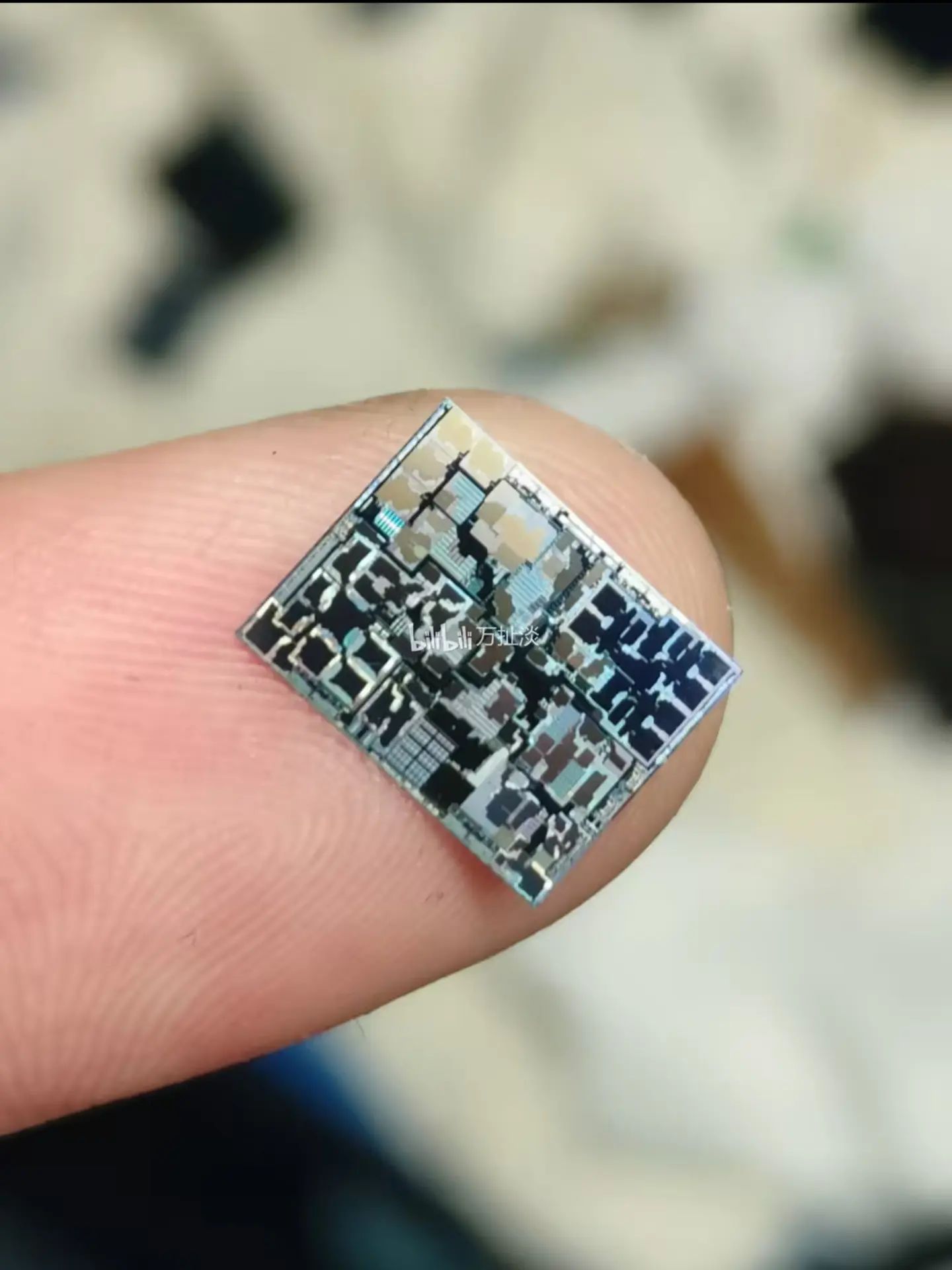
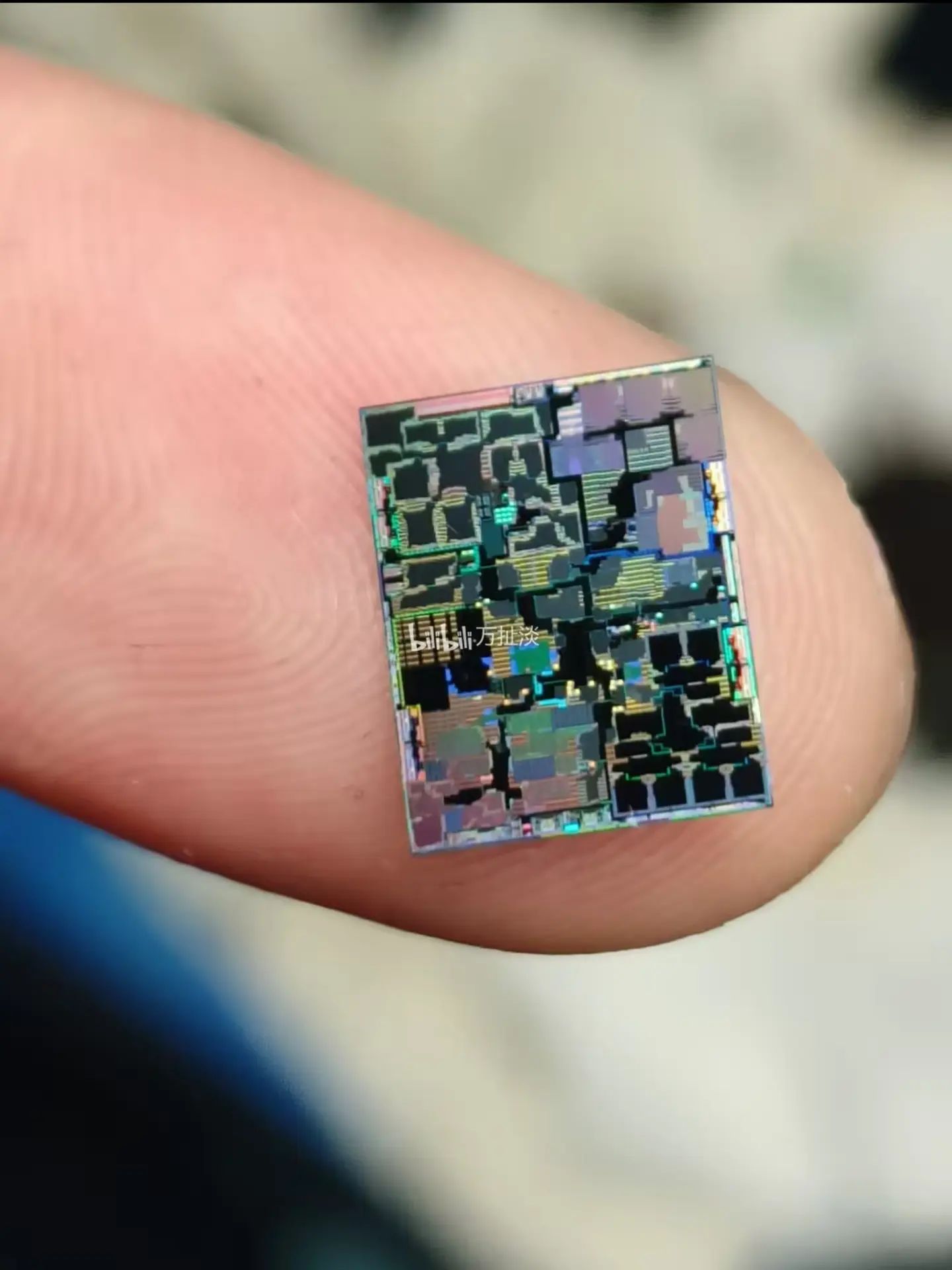
Semiconductors are among the most intricate products crafted by humans, demanding substantial investments, extensive research and development, pinpoint accuracy, and a broad spectrum of expertise. Examining semiconductors up close, particularly from within, offers a fascinating glimpse into their complexity and functionality.
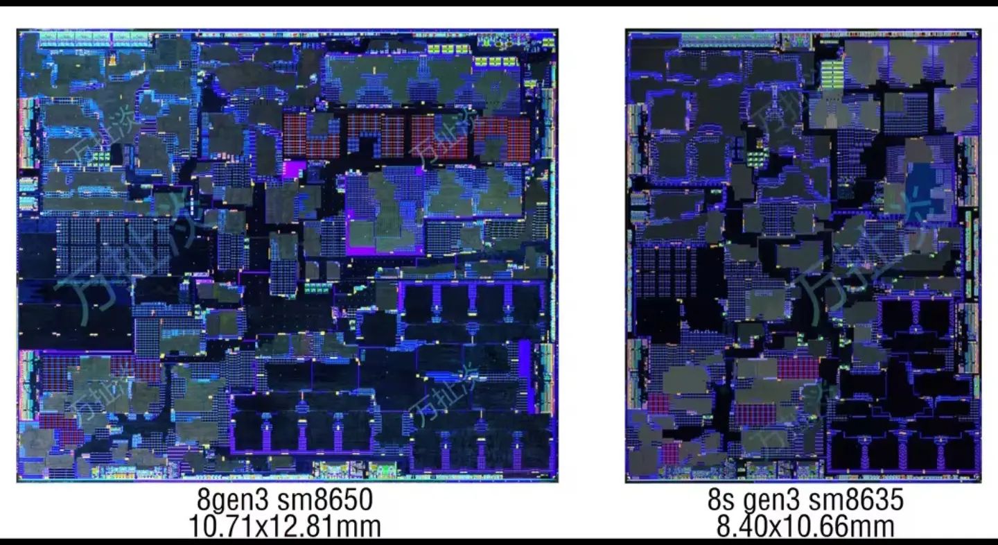
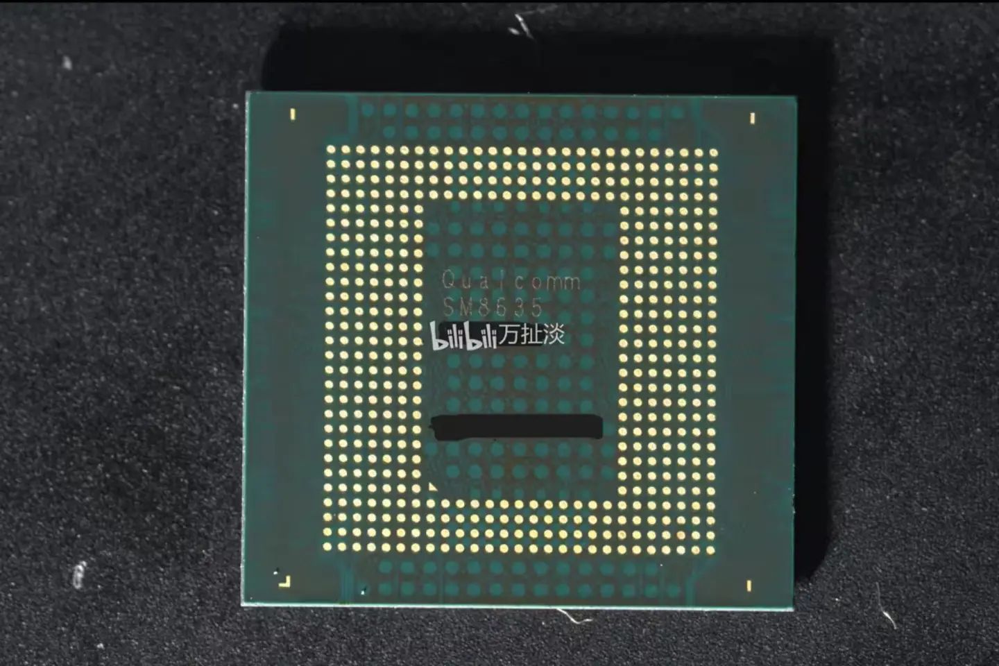
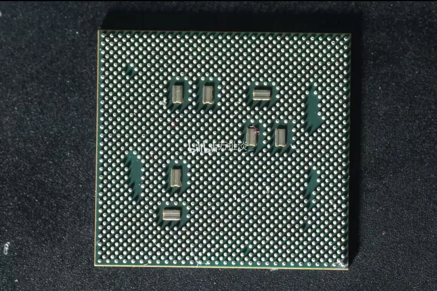
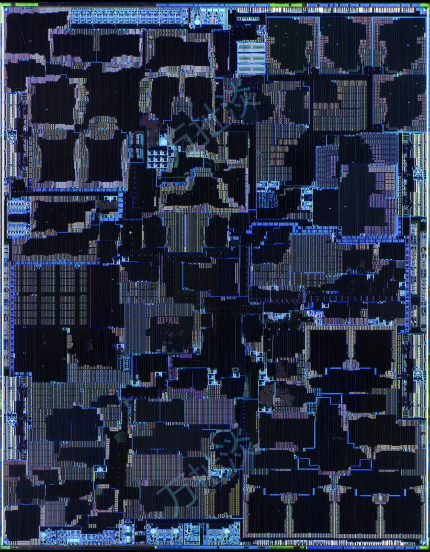
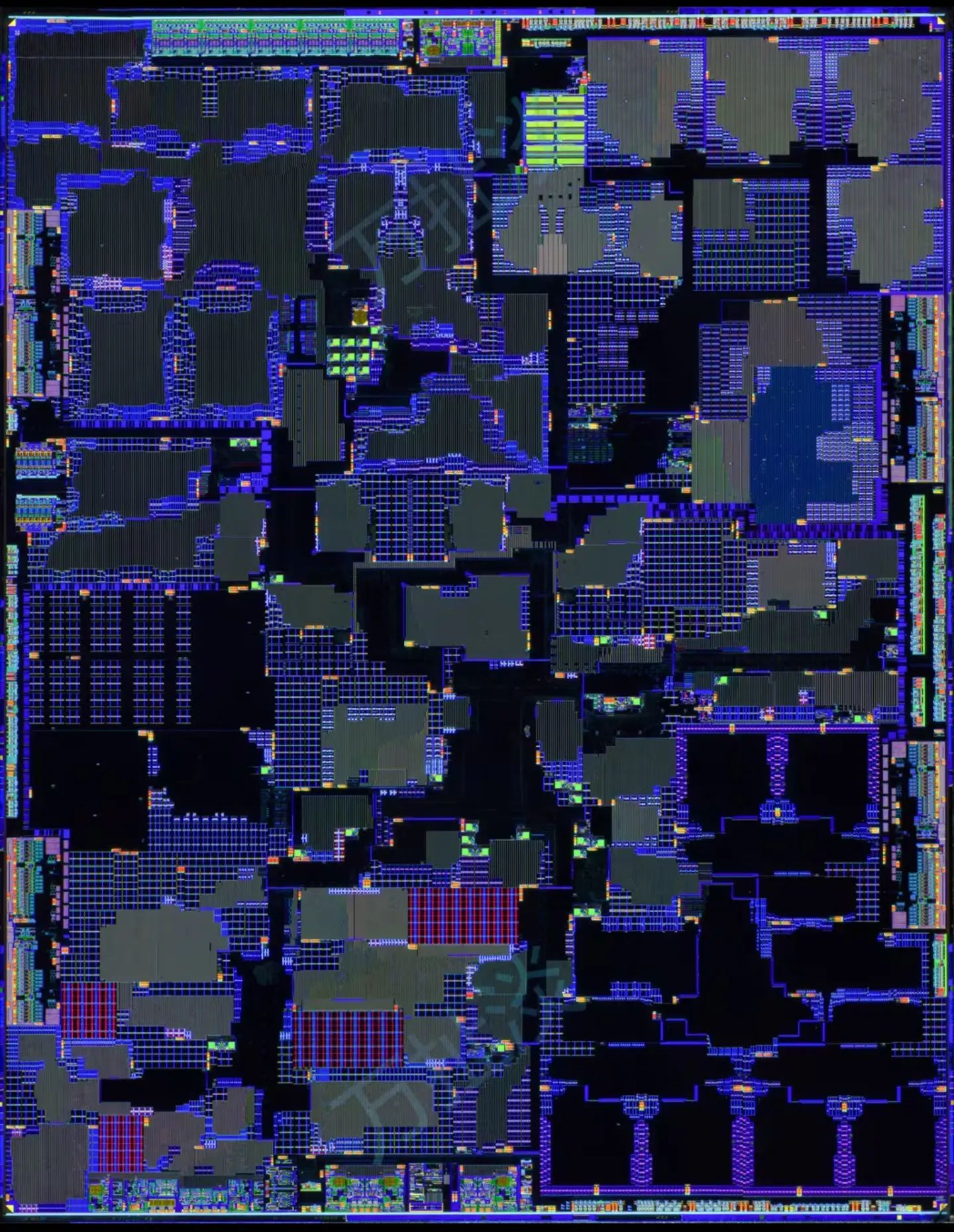
Recently, Wàn Chědàn, a master of semiconductor disassembly, shared newly published images detailing the internal design diagram of the latest Snapdragon 8s Gen3 chipset. Despite belonging to the same series and employing TSMC’s 4nm process, there are notable disparities between the Snapdragon 8s Gen3 and the Snapdragon 8 Gen3 chipsets.
In dissecting the pictures, it’s revealed that the actual chip size of the Snapdragon 8s Gen3 measures only 8.40 × 10.66mm, compared to the 10.71 × 12.81mm dimensions of the Snapdragon 8 Gen3. This indicates a difference of approximately 35 percent, prompting a closer examination of the technical specifications.
The Snapdragon 8 Gen3 utilizes TSMC’s 4nm process and boasts a 1+3+2+2 four-cluster CPU architecture. This setup comprises a 3.3GHz X4 core, three 3.15GHz A720 cores, two 2.96GHz A720 cores, and two 2.26GHz A520 cores, alongside an Adreno 750 GPU.
Conversely, the Snapdragon 8s Gen3 also harnesses TSMC’s 4nm process but adopts a 1+4+3 CPU architecture. This configuration includes one 3GHz X4 core, four 2.8GHz A720 cores, three 2GHz A520 cores, and an Adreno 735 GPU. Notably, the Snapdragon 8s Gen3 features one less A720 core and one additional A520 core in its CPU section compared to the Snapdragon 8 Gen3, along with differing frequencies.
In terms of cache, adjustments are evident. The X4 mega-core’s L2 cache has been reduced from 2MB to 1MB, the A720 mega-core’s L2 cache from 512KB to 256KB, the L3 cache from 12MB to 8MB, and the SLC cache from 6MB to 3.5MB.
On the GPU front, the Snapdragon 8s Gen3’s Adreno 735 slots in between the Adreno 730 of the Snapdragon 8 Plus Gen1 and the Adreno 740 of the Snapdragon 8 Gen2. Notably, the number of cores has been halved from 6CUs to 3CUs, with 1,536 ALUs reduced to 768 ALUs, albeit with an increased frequency of 1,100MHz.
Upon analysis, it appears that the Snapdragon 8s Gen3 likely matches or slightly surpasses the performance of the Snapdragon 8 Gen2, primarily due to its more potent CPU. However, its GPU capabilities may not reach the same level of excellence.